Case study
Hitachi High-Technologies (Europe)
When Japan’s Hitachi Group chose Sci-Tech Daresbury to create a brand new applications lab for their latest Scanning Electron (SEM) and Atomic Force Microscopes (AFM), it emphatically underlined the campus’ credentials as one of the UK’s leading innovation centres.
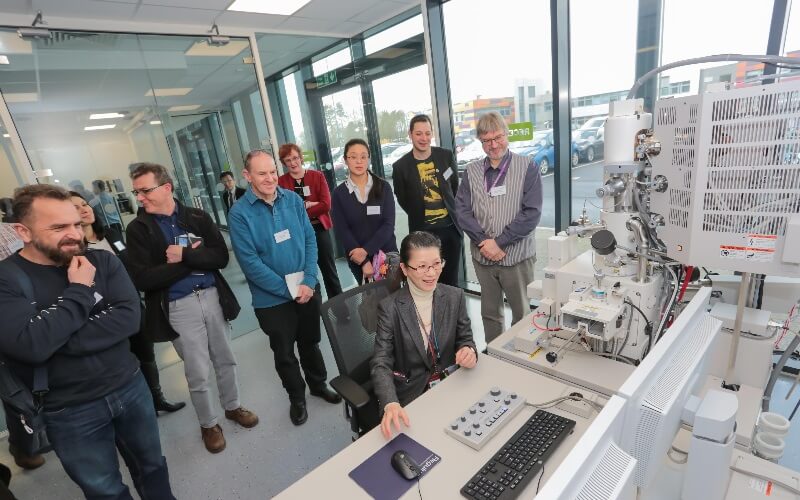
Hitachi High-Technologies (Europe) took 2,500 sq. ft. of laboratory space in the campus’s newest building, Techspace One to create a suite of dedicated microscope rooms.

Sci-Tech Daresbury an attractive prospect
According to Mike Dixon, Hitachi High-Technologies (Europe) Microscopy Section Manager UK/Ireland, Sci-Tech Daresbury was attractive prospect for several reasons: “What really appealed about Techspace One was its strong impact and flexibility, allowing us to design the space in the way that works for us best. The move also meant that we were able to add new staff to strengthen the company’s applications and technical team, and in so doing increase our commitment to microscopy in the UK.
“Also, locating at Sci-Tech Daresbury has put us in the heart of the UK, offering opportunities to work with academic and industrial partners on the campus and in the region, as well as across the whole of the UK and Europe because of the excellent transport links.”
Hitachi High-Technologies’ new laboratory is capable of undertaking a wide range of studies giving insights into the structural, chemical and crystallographic properties of materials. Electron microscopy offers the ability to provide more spatially-resolved chemical information than other techniques, allowing scientists and engineers to understand exactly what element is where, right down to a nanometre scale. Scanning probe microscopy offers the ability to understand and quantify the electrical, mechanical and magnetic properties of materials, also down to the nanometre scale.
Mike Dixon, added: “Our new laboratory is a demonstration facility and collaboration hub where we undertake fundamental research, method development and proof-of-concept case studies using our latest techniques. Our advanced sample preparation, SEM and AFM solutions are widely used in the nanotechnology industry for materials development, quality control, failure analysis and industrial forensics.”
The international leading–edge technology company, which has centres of excellence across Europe, has settled in quickly and has established strong relationships with others on the campus including with the renowned EPSRC National Facility for Aberration Corrected Scanning Transmission Electron Microscopy (“SuperSTEM”).


